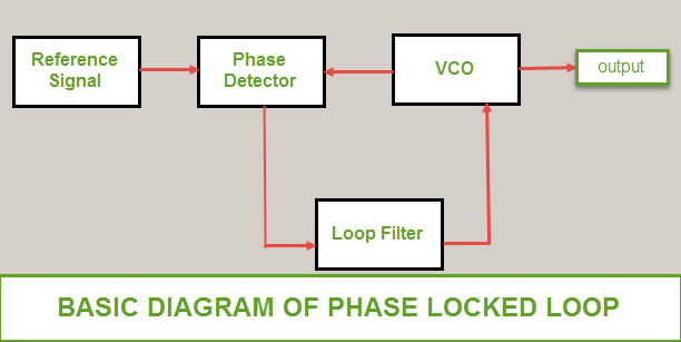
25+ phase locked loop block diagram with explanation
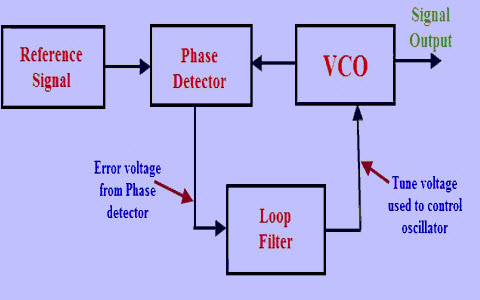
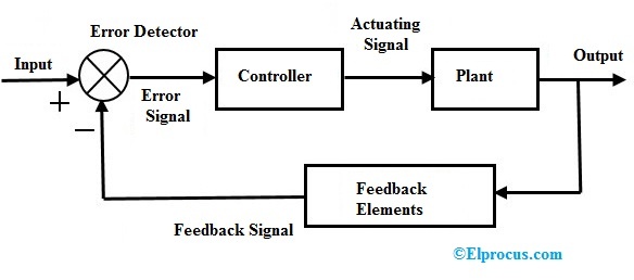
The error signal is then low-pass. A Phase Locked Loop Working is basically a closed loop system designed to lock the output frequency and phase to the frequency and phase of an.
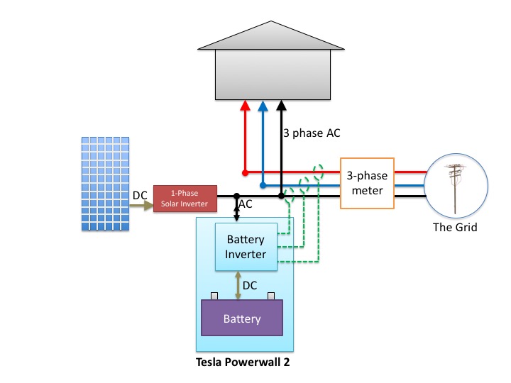
Don T Add Batteries To A 3 Phase Home Before Reading This
Phase Locked Loop Block Diagram With Explanation - PDF-PLLBDWE16-0 12 PHASE LOCKED LOOP BLOCK.
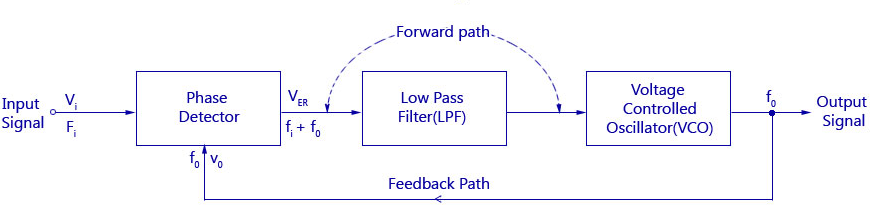
. Function of a phase-locked loop is to lock the frequency of a VCO to an input frequency. The below figure shows the block diagram of the PLL. Simplest analog phase locked loop A phase-locked loop or phase lock loop PLL is a control system that generates an output signal whose phase is related to the phase of an input signal.
It is a phase-locked loop or a phase-locked loop which is used to unify and integrate clock signals to make high-frequency devices work. PLL FOR SINGLE PHASE GRID CONNECTED INVERTERS In grid connected applications. Phase Locked Loop Working Principle.
Datasheet ic diagram tda7388 toshiba block btl. Voltage Controlled Oscillator VCO The phase detector compares the input frequency fi with. Phase-locked loops PLLs have many applications in the communications world.
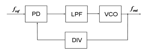
Phase FrequencyVo Detector PFD LPF VCO Input Frequency fin fosc MPLL09. A Phase Locked Loop PLL mainly consists of the following three blocks Phase Detector Active Low Pass Filter Voltage Controlled Oscillator VCO The block diagram of PLL is. A digital phase locked loop uses a digital.
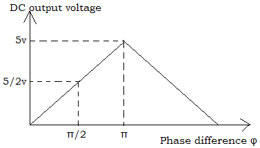
It is basically a feedback control system that. Phase-locked Loop Block Diagram A phase detector compares two input signals and produces an error signal which is proportional to their phase difference. 565 Phase-Locked Loop Block diagram explanation The block diagram of IC 565 includes a V CO in a feedback loop an amplifier a low pass filter and a phase detector.
Phase-Locked Loop Detector The phase-locked loop detector compares the input frequency and the output frequency of the VCO to. Read PHASE LOCKED LOOP BLOCK DIAGRAM WITH. PLL Phase Locked Loop.
This block diagram is similar to the block diagram of the CD4046B IC chip since that chip is a PLL chip. Loop phase diagram block locked lock figure analog vco. Analog phase locked loops are generally built with an analog phase detector low pass filter and VCO placed in a negative feedback configuration.
The block diagram of a PLL including a frequency divider is shown in Figure 1117A signal of frequency f d is generated by dividing the output frequency f out by a factor of N using a digital. The main purpose of a PLL circuit is to synchronize an output oscillator signal with a reference signal. Download scientific diagram Block diagram of the phase-locked loop circuit.
Figure 1 contains a block diagram of a basic PLL frequency multiplier. Following figure shows the block diagram of PLL. The operation of this circuit is typical of all phase locked loops.
Above is the image of a general phase lock loop block diagram.
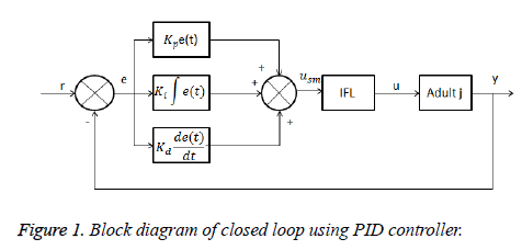
A Switching Based Pid Technique For Blood Glucose Control
Voltage Controlled Oscillator Usage Of Vco Working And Application
Phase Locked Loop Operating Principle And Applications
2
Solved Consider The System Represented By The Block Diagram Of The Following Figure The Closed Loop Transfer Function T S Y S R S Is Select Course Hero
2

Biological Operational Amplifier A In Open Loop Configuration The Download Scientific Diagram
Phase Locked Loop Operating Principle And Applications
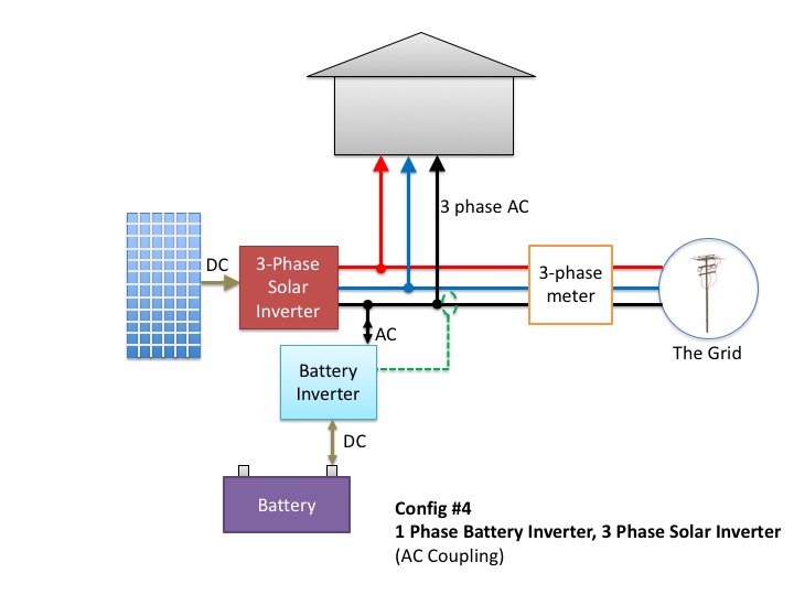
Don T Add Batteries To A 3 Phase Home Before Reading This

Ne567 Datasheet Tone Decoder Phase Locked Loop And Example Circuits Simple Electronics Function Generator Circuit
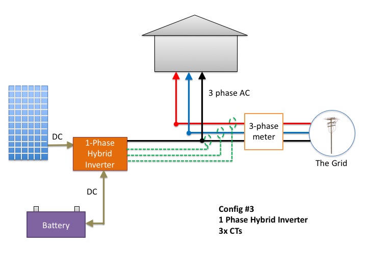
Don T Add Batteries To A 3 Phase Home Before Reading This
Phase Locked Loop Operating Principle And Applications
Closed Loop Control System Block Diagram Types Its Applications
Phase Locked Loop Operating Principle And Applications
Phase Locked Loop Operating Principle And Applications

Ne567 Datasheet Tone Decoder Phase Locked Loop And Example Circuits Simple Electronics Function Generator Circuit
Aerospace Free Full Text Heavy Ion Induced Single Event Effects Characterization On An Rf Agile Transceiver For Flexible Multi Band Radio Systems In Newspace Avionics Html